In order to satiate a growing desire to incorporate my musical interests into my technical projects, I arrived at a new project idea that would satisfy both: A DIY audio DSP module. Currently, the idea is to build it into a guitar pedal, and provide a software interface for creative routing and interconnection of various audio effects, all implemented through digital logic on an FPGA.
The first step of achieving this was to find some way to turn the analog audio signals coming from my instrument(or any other source) into digital ones, to which I could apply my DSP magic. I would also need a way to turn those modified digital signals back into analog audio once again.
Rather than looking for some off the shelf solution, I decided to get my hands dirty with some PCB design. It’s been a while.
Doing what any good maker would do, I hopped on DigiKey and picked out both a D/A and an A/D chip that satisfied my needs: The cheapest possible thing that can handle 24-bit, 44.1kHz (which is good enough for rock’n’roll in my opinion) with minimal supporting circuitry. Settling on the PCM1808 from TI for the A/D, and the NAU8402 from Nuvoton for the D/A. I also had to source a special PLL to generate the audio-specific clock signals required. Basing my design heavily on the reference designs given in each respective datasheet, I put together a simple board with some 2.54mm pin headers for easy connection to whatever I need.
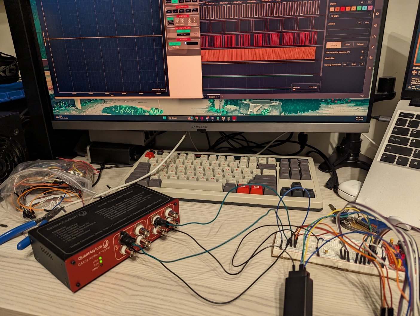
Somehow, the board actually worked first try, which I think is a first! All I needed to do was change a solder bridge to ensure the correct clock frequency was generated, and the right control signals were connected. My test procedure was to first connect the output of the A/D directly to the D/A, and see if audio would be passed through. I was able to carefully verify this with a QuantAsylum QA401 audio analyzer that I had recently acquired during my time at Untether (it was lying around the office with no clear use, so they gave it to me). I was also able to make detailed frequency response measurements, which appear to be very flat despite the jankiness of my test setup.
My next step was to connect all of the signals to the FPGA, and ensure that the converters could be controlled and read by the FPGA. The FPGA drives all of the necessary control signals to the correct state, and at first, I just assigned the input to the output to create another passthrough, this time with the FPGA in the middle. This also worked.
Since I am now confident that my analog frontend is functional, I need to get to implementing the actual DSP. Much research and learning will be required- I think after I finish ECE 313 this term I’ll have a good idea of the DSP algorithms, and I also have picked up a textbook on implementing those on FPGA, so i’m well on my well. I also need to implement an I2S encoder/decoder state machine to interface with the PCM audio signals properly.
Preliminary Verilog code can be found in this repo, and schematic design files can be found in this one.