Another project I was tinkering with over the Winter 2024 term, was integrating the SM83 core from VerilogBoy into a project with my old Spartan-6 FPGA board. I had an idea that had come to me while I was attempting to do my own FPGA emulation of the SM83 core: Wouldn’t it be cool if I could do some modern computing tasks with such an old and simplistic CPU core as the one behind the original Game Boy? I figured why not make an 8-bit microcontroller, complete with a UART bootloader, GPIO, and maybe even I2C and SPI, for all kinds of fun projects? There isn’t a particular advantage to having such a microcontroller, but I though it would be a fun and interesting challenge, all while scratching my nostalgia itch. There may in fact be advantages to such a simplistic core being used, such as minimal power/area usage, but those could be explored once the project is more mature.
I would have loved to tackle this with my own SM83 core I built from scratch, but I was starting to lose steam with that project, and there is still a lot of work to do. Making use of the core from VerilogBoy would allow me to “shift left” (a term coined by my manager at Untether) my development and start working on the next task before my core was finished. I had also gotten a fair taste of cpu architecting and RTL design from my work with LETC, and from the lessons learned there I was realizing that I might want to completely restructure the core again from the ground up.
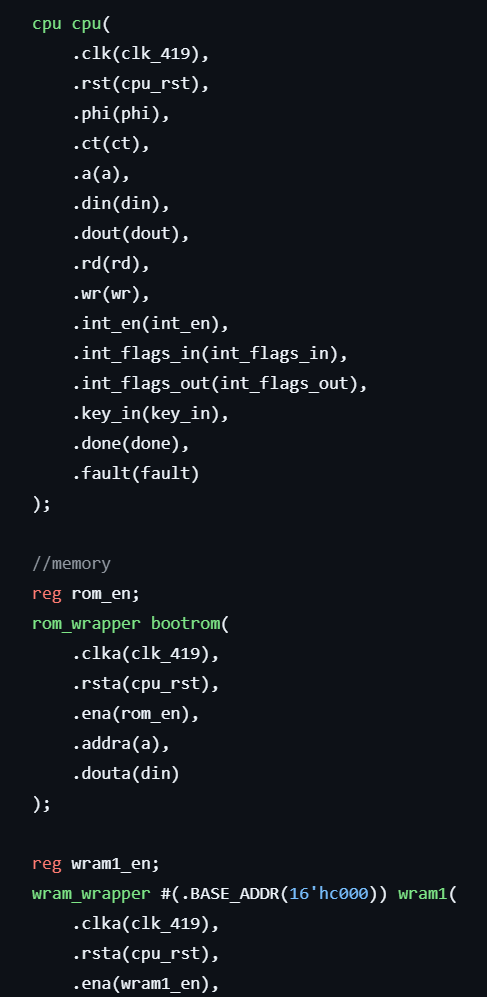
After instantiating the VerilogBoy core in my top level module, I created a simple testbench that would drive the right control signals and start execution. I have been making use of the memory IPs provided by Xilinx through the ISE IDE, so it wasn’t a lot of effor to get some block memory up and running and load it with program code. I simply had to take the assembled gameboy binaries (created via rgbds, which is a fantastic retro assembler project with excellent documentation) and convert them into a simple list of bytes (in the .coe file format) via a python script, so that the IP generator could synthesize the memory to be initialized with the program code.
Upon running the test bench, I could see the core happily executing instructions.
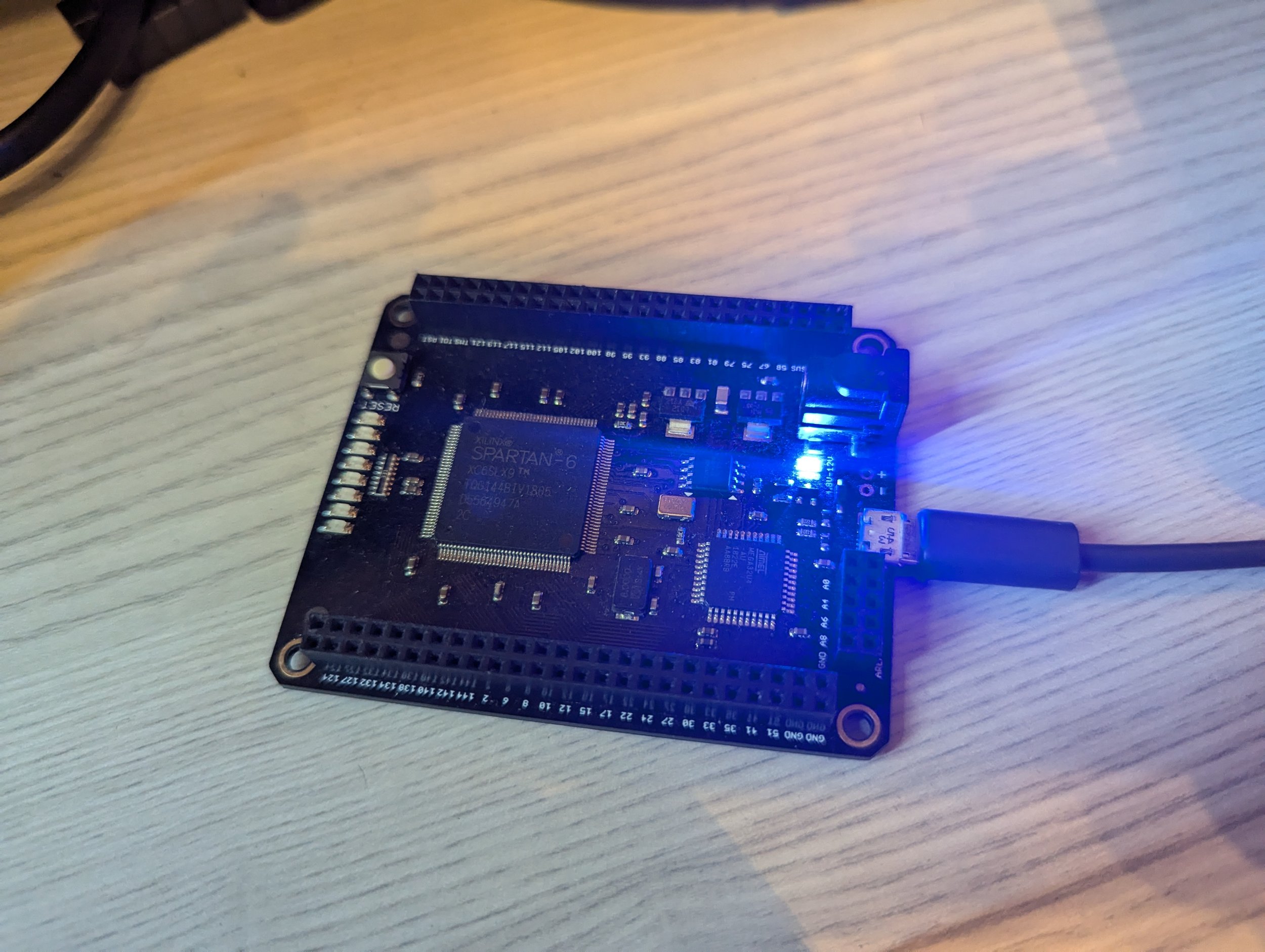
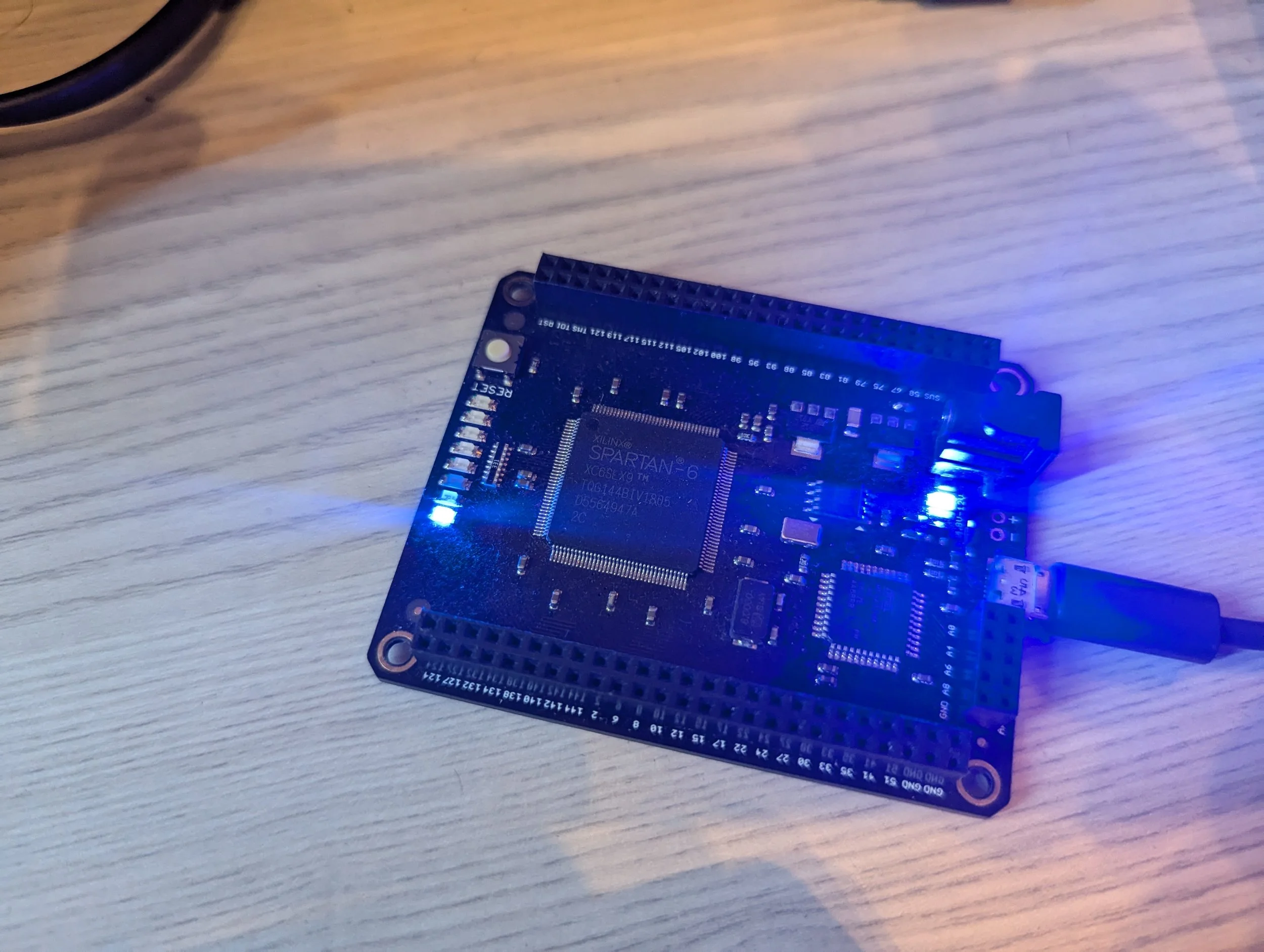
Next order of business was to get things working on the actual board. This was a matter of instantiating the core and the memory inside the top level file for synthesis, get the correct pin assignments in place, and connect the clock signals. I also used Xilix’s clock divider IP to generate a clock signal that would be appropriate for driving the SM83 core. (I at first tried to generate a 4.19 MHz clock that would be faithful to the original Game Boy). I wrote and assembled a simple blink program that would run a busyloop and blink one of the on-board LEDs every half-second or so, just to confirm that the core was up and running and executing code. This seemed to work without a hitch.
After the blink code was running, I moved on to trying to get the UART to work. I decided to create a simple memory-mapped peripheral interface, using the provided UART functions that came with the example code for the board (I didn’t want to muck around with rolling my own here, as the board manufacturer has their own tricky firmware inside the AVR that interfaces with the USB connection, which is also used to configure the FPGA.) Looking at the Game Boy’s memory map (credit to Pan Docs), there is a small blank space at 0xFEA0 to 0xFEFF that Nintendo says is not useable. We’re not Nintendo however, so we’re gonna use it for the UART control registers.
I came up with a bog standard setup for a simple SISO UART interface: Two bytes for control and status bits, One byte for TX, and one byte for RX. After hacking up the provided AVR interface RTL to add in these data and control registers, I could instantiate it in my top module and attempt to use them.
It took a little bit of messing around to get this working. Everything I did in the Verilog made sense, but I was stuck for a while due to a few mistakes. One: The baudrate was hard-calculated based on a 50MHz clock, which wasn’t quite working correctly with the seperate clock domain I had created for the SM83 core, so I had to move the AVR module into the same clock domain, and make sure the baudrate was being calculated correctly. I also was trying to use 115200 baud, which seemed reasonable, but the problem is that the firmware in the AVR is hardcoded to use 9600, so no matter what I did in the Verilog could affect that. After I ironed out all of these problems, I was greeted with the glorious sight of several “@” symbols being printed on the UART.
Next, I wanted to try to get some semblance of a bootloader working, as I was getting tired of having to synthesize the FPGA image over and over again every time I wanted to iterate on the program code.
This would require SRAM, so I quickly used the IP core generator to create some LUTRAM that would live at the correct memory locations corresponding to the original Game Boy’s work ram (since it was a cartridge based system, I don’t think the work RAM was ever used for program code, but there’s a first time for everything!)
So I attempted to compose a crude bootloader with the following behaviour:
Print a ready character every second until the programmer sends a start character. (I chose @ and *)
Consecutively write each byte to memory starting at the beginning of work ram
Print the contents of memory written so far when a special character is received (I chose “/”
Jump to the beginning of work ram and execute the code when another special character is received (I chose “!”)
I understand that there are myriad issues with this approach, but for a proof of concept, it’s fine.
I was stuck getting this to work for a long time as well- still a novice with FPGA, I had been ignoring a certain warning at the end of synthesis that I knew I shouldn’t be: I was violating timing. The issue turned out to be that I was trying to use this obscure non-standard clock frequency with the clock divider. This led the clock IP to behave weirdly and generate an unreliable clock signal for all of the components, causing the memory to randomly be corrupted while I was trying to upload.
After sorting this out, I was able to very crudely write my program code one byte at a time into RAM using a serial terminal. The program code would simply display a specific pattern on the onboard LEDS (directly connected to another sneaky register I added to Nintendo’s memory map).
Which is as far as I’ve gotten- next steps will be to automate the bootrom flow for uploading more complex programs, and begging to integrate various peripherals. Stay tuned!